Superconductivity breakthrough could unlock ultra-efficient electronics
Swedish researchers showed that a carefully patterned interface can help an ultrathin superconducting layer tolerate higher temperature and strong magnetic fields, but it remains a lab result rather than a finished electronics platform.
Jonah Reed ·
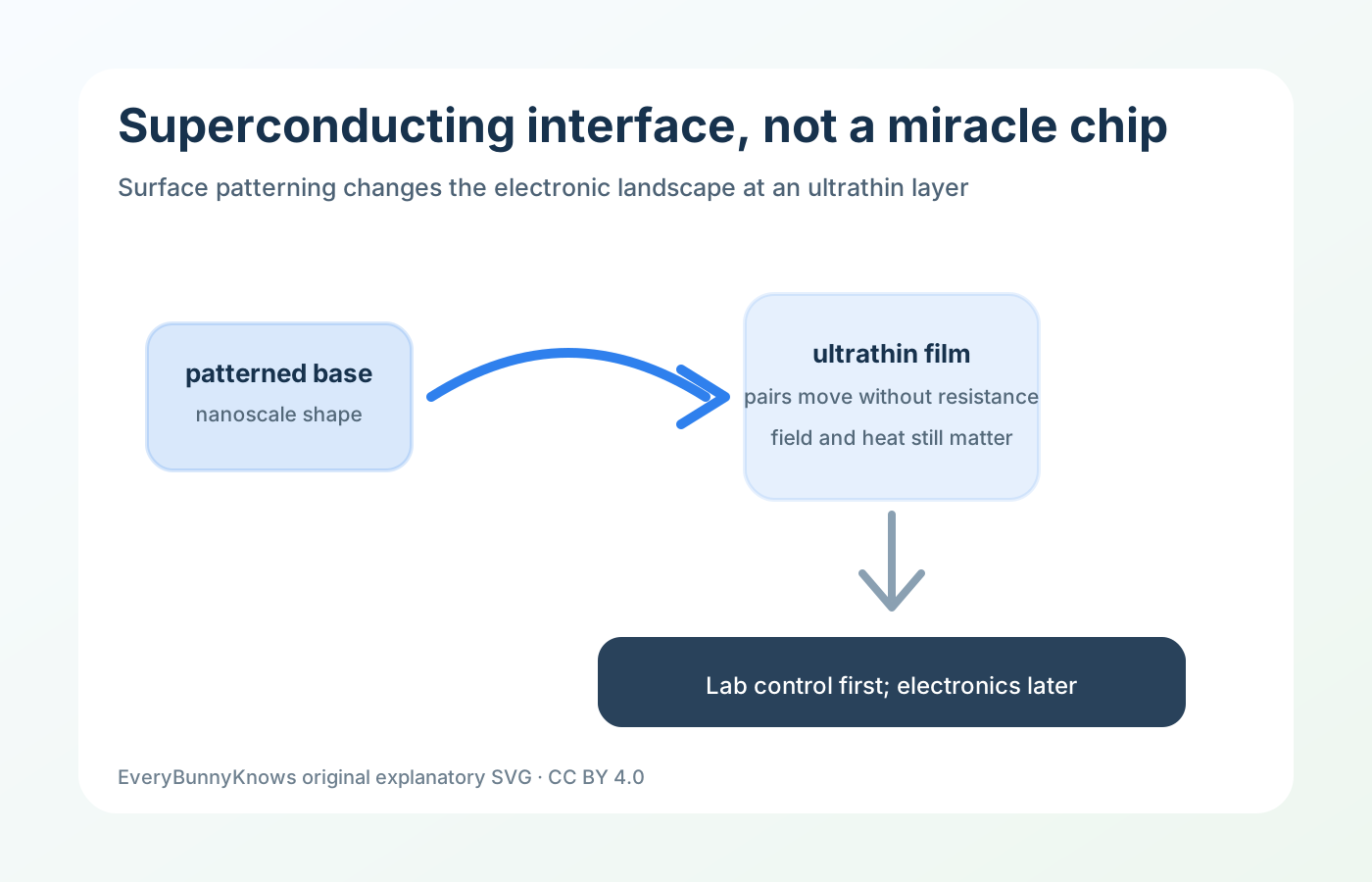
A superconductivity result from Sweden is worth reading carefully because its promise is specific. The Chalmers University of Technology team around Riccardo Arpaia reported that an ultrathin superconducting material behaved better when the surface beneath it was subtly shaped at the nanoscale. The point is not that ordinary phones or data centers are suddenly about to run on room-temperature superconductors. It is that a boundary only a few atoms thick can be engineered so the fragile superconducting state survives under warmer and harsher conditions than the same material would otherwise tolerate.
The mechanism sits at a boundary only a few atoms thick. In a superconductor, paired electrons move through a material without electrical resistance, but heat and magnetic fields tend to break that ordered state. In this work, the patterned support changes the electronic landscape at the interface. That can alter how charge carriers line up, how vortices form in magnetic fields, and how the layer holds together when the usual disruptions appear. In plain language, the shape below the film becomes part of the device physics, not just a passive holder.
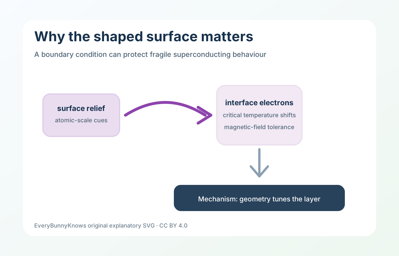
That is why the result matters for electronics. Resistance wastes energy as heat in interconnects, sensors, memory elements and specialized quantum circuits. Superconductors can remove that loss in principle, but most practical systems still need cooling, careful materials processing and protection from fields or defects. A method that raises the usable window of an ultrathin film could make future components easier to integrate, especially where small devices already operate in controlled cryogenic environments.
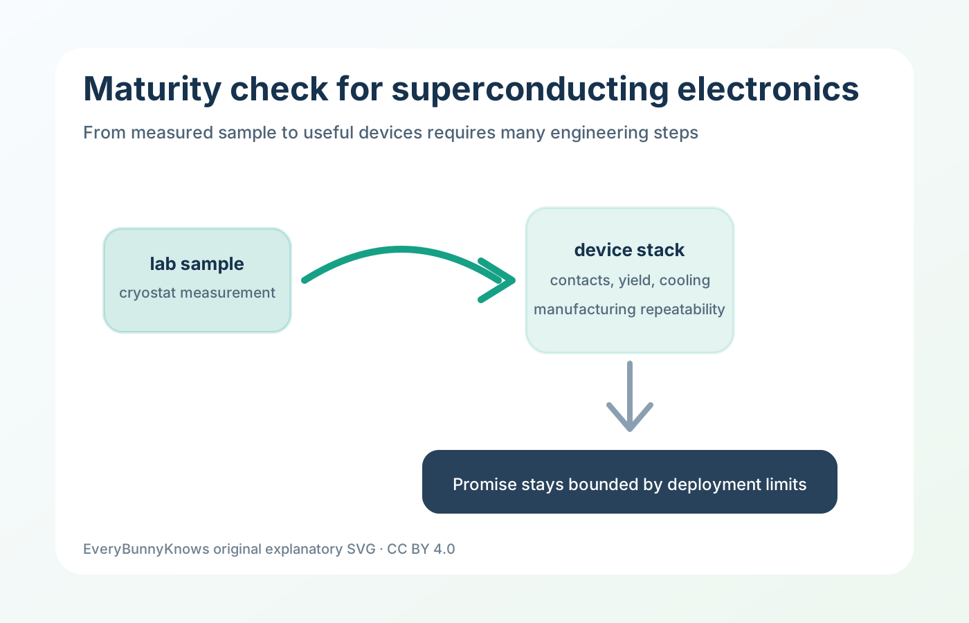
The evidence should also be kept in scale. This is a laboratory materials result, not a manufacturing recipe for consumer chips. The next questions are repeatability, contact resistance, wafer-scale growth, long-term stability, device yield and whether the same interface idea works with other compounds. Even a real improvement in critical temperature or critical field does not erase cooling hardware, packaging constraints or the cost of making atomically clean layers.
The hopeful part is therefore quieter than the headline. Researchers are learning to tune superconductivity by designing the neighborhood around a material, not only by searching for a perfect new compound. If that control becomes reliable, it could feed sensors, quantum devices and low-loss electronics one carefully measured interface at a time.
A good way to read the result is through the engineering chain. First comes the surface pattern, then the ultrathin film, then low-temperature measurement, then a possible device geometry. Each step can introduce defects or costs. The study is valuable because it identifies one controllable link in that chain: the interface. It does not remove the need for better fabrication, but it gives researchers a knob they can deliberately turn instead of treating the supporting surface as background.
That also keeps the social meaning realistic. Ultra-efficient electronics would matter because computing, sensing and communication all lose energy as heat. Yet the first beneficiaries of improved superconducting films would probably be specialized instruments, quantum hardware and research devices, not household gadgets. The path from an elegant sample to broad public benefit is long, but it begins with mechanisms that can be measured and repeated.
For readers, the practical test is whether the mechanism changes decisions. A credible technology story should say what has been measured, what still belongs to prototypes, and which real-world system would have to change before the idea matters outside a paper. That discipline keeps optimism useful: it points to next experiments, standards, operators and costs instead of treating a promising result as a finished product.